From Silicon to Signal: The Hidden World of Analog Front-End (AFE) Design In a world ruled by digital technology, the path from signals in the real world to digital information starts in a location that few even grasp—the analog front-end (AFE). This pivotal block of circuitry occupies the location where physical phenomena meet compute capability and is central to precise sensing and measurement in markets ranging from medical electronics and industrial automation to instrumentation systems.
Let's venture into the uncharted realm of AFE design and see what makes op-amps, filters, and ADCs combine to create the accuracy backbone of today's electronics.
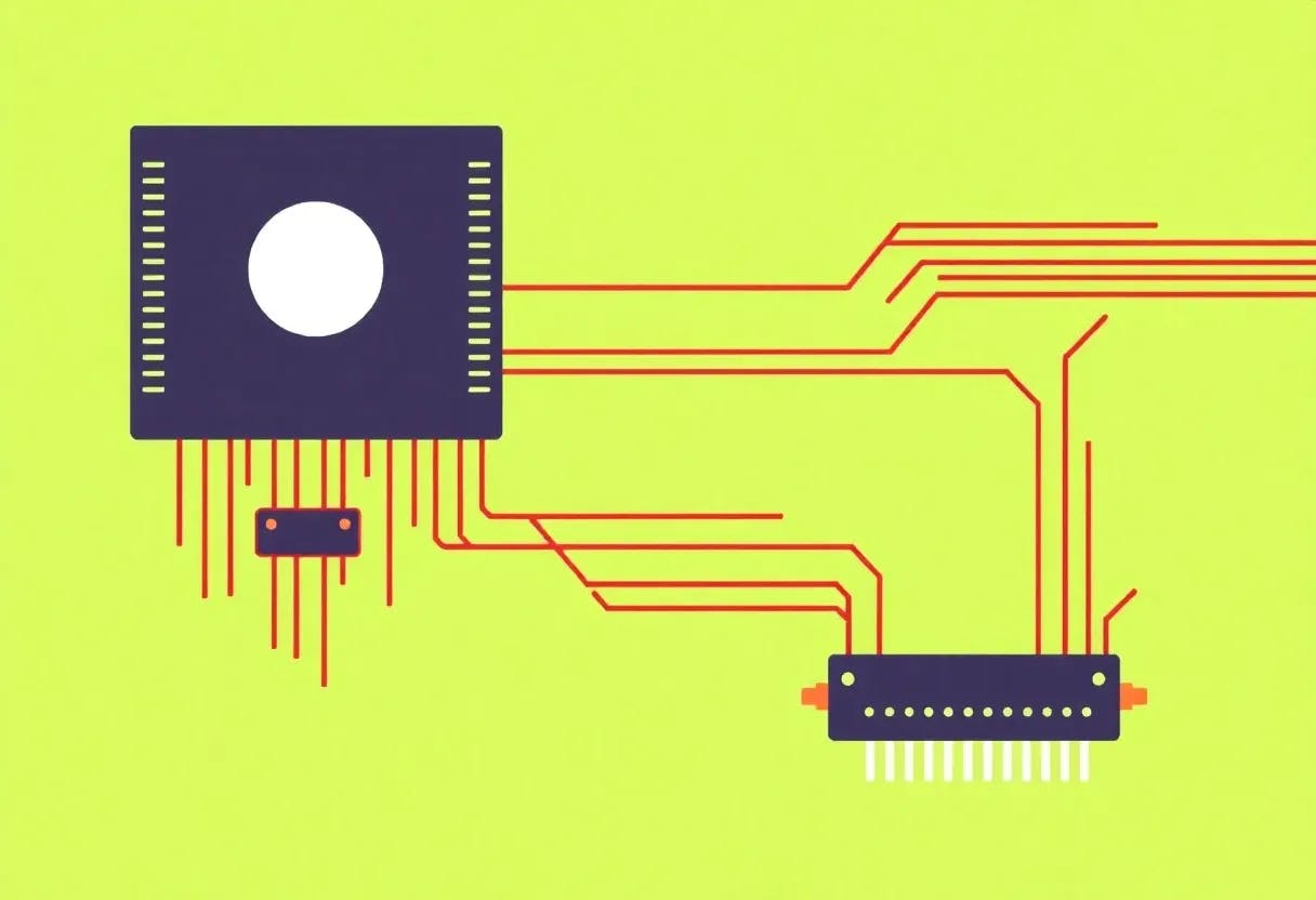
What is an Analog Front-End?
An Analog Front-End (AFE) is a signal-conditioning system that's used to capture, filter, and amplify analog signals prior to them being converted into digital signals. Such signals, quite commonly originating from sensors or transducers, tend to be low-level and noisy—meaning they need specialized handling before they can be processed by a microcontroller or digital signal processor (DSP).
An AFE essentially gets the signal ready for the shift from the analog realm to the digital world. Core Elements of an AFE Circuit Designing an AFE requires choosing and optimizing a number of interdependent analog building blocks, each designed to maintain signal integrity across a variety of noise and bandwidth constraints.
-
Low-Noise Operational Amplifiers (Op-Amps) Central to most AFEs is the op-amp. It's employed for signal amplification, buffering, and filtering. Input-referred noise: Particularly critical in low-signal applications such as ECG or seismic monitoring. Gain-bandwidth product (GBW): Must equal the frequency characteristics of the signal. Offset voltage and drift: Essential for long-term accuracy and temperature stability. Femtoamp input bias currents and nanovolt noise floors are typical in medical and scientific apparatus.
-
Analog Filters Signals need to be filtered of unwanted frequency content before being converted to digital. Low-pass filters (LPF): Block high-frequency noise and aliasing in ADCs. Band-pass filters (BPF): Filter signal bands, applied in applications such as EEG or vibration sensing. High-pass filters (HPF): Remove DC offsets or baseline drift. Most filters are designed with RC networks and op-amps (active filters) for the sake of accuracy.
-
Analog-to-Digital Converters (ADCs) The last stage of the AFE converts digital bits from analog signals. Resolution (bits): Defines the level of detail at which a signal is quantized—higher resolution for better measurements. Sampling rate: A minimum of twice as high as the highest signal frequency (according to Nyquist theorem). Input voltage range: Compatible with the output swing of the previous analog stage. Architecture: SAR (Successive Approximation Register) ADCs for moderate-speed, high-resolution applications; Sigma-Delta for low-speed, ultra-high-precision applications. ADC Architecture Comparison
|
Feature |
SAR ADC |
Sigma-Delta ADC |
|---|---|---|
|
Speed |
Moderate (up to ~10 MSPS) |
Low (typically <1 MSPS) |
|
Resolution |
Up to 18 bits |
Up to 24 bits |
|
Power consumption |
Low to moderate |
Low (but higher latency) |
|
Applications |
Industrial control, battery monitoring |
Medical sensing, audio, precision instrumentation |
|
Complexity |
Simple |
More complex, requires decimation filters |
Critical AFE Design Considerations
Signal Integrity and Impedance Matching
AFE circuits need to preserve signal integrity when handling high-impedance sensors or extended cable lengths. It is imperative to use buffering stages and optimal impedance matching to avoid signal attenuation.
Common-Mode Rejection and Grounding
Instrumentation amplifiers and differential signal acquisition reject common-mode noise—especially in noisy electric environments. Effective PCB grounding schemes (star grounding, ground planes) are necessary to ensure minimal hum and ground loops.
PCB Layout and Noise Immunity
AFE performance can be ruined by bad layout. Methods involve:
- Short trace lengths
- Accurate decoupling of power rails
- Isolation of analog and digital grounds
- Shielding sensitive analog traces from EMI
- Minimizing Noise in AFE Design
Noise is the archenemy of precision. AFE designers need to consider several sources of noise:
- Thermal noise: Inherent to resistors and conductors.
- Flicker noise (1/f noise): Relevant in low-frequency measurements.
- Quantization noise: Added during ADC conversion.
- Environmental noise: From switching regulators, wireless signals, or other digital circuits nearby.
Solutions are low-noise components, shielded enclosures, and adequate filtering.
Minimizing Noise in AFE Design
Noise is the nemesis of precision. Several noise types must be mitigated:
- Thermal noise: From resistors and semiconductors.
- Flicker noise (1/f): Dominant at low frequencies.
- Quantization noise: Introduced during digitization.
- Environmental noise: From switching power supplies, RF interference, etc.
Mitigation strategies include choosing low-noise components, isolating sensitive analog paths, and using EMI shielding.
Design Trade-Offs in AFE Development
Every AFE design must strike a balance among competing requirements:
|
Trade-Off |
Description |
|---|---|
|
Noise vs. Power |
Low-noise designs often require more power for amplification and filtering. |
|
Resolution vs. Speed |
Higher resolution ADCs usually have slower conversion rates. |
|
Integration vs. Flexibility |
Integrated AFEs reduce size and cost but may sacrifice customizability. |
|
Cost vs. Performance |
Precision op-amps and high-resolution ADCs come at a premium. |
Designers must tailor these trade-offs to suit the application’s constraints—whether it’s battery life in wearables or bandwidth in radar systems.
Case Study: AFE for Biomedical Instrumentation
For an ECG (electrocardiogram) monitoring system, for example. The AFE is required to:
-
Process microvolt-level signals from the human body.
-
Have high common-mode rejection (usually > 100 dB).
-
Prevent patient current leakage (safety standards such as IEC 60601).
This arrangement could employ an instrumentation amplifier, active band-pass filter (0.05–100 Hz), and high-resolution sigma-delta ADC—demonstrating the subtlety of the engineering.
Broader Application Domains
Beyond biomedical applications, AFEs serve across various industries:
-
Automotive: Sensor data for ADAS, tire pressure monitoring (ISO 26262)
-
Aerospace: Vibration analysis, inertial navigation
-
Environmental monitoring: Air quality sensors, water pollution analyzers
-
Industrial automation: Motor control feedback, robotic joint sensing (IEC 61000 for EMC compliance)
Each application demands a unique combination of noise immunity, speed, accuracy, and reliability—highlighting the versatility of AFE design.
Utilization of AFE Design in Transportation
The transportation industry increasingly relies on precise signal processing and real-time monitoring, both of which are facilitated by AFE technology. Key applications include:
Key Applications
-
Vehicle Sensing and Control
-AFEs are critical in processing signals from sensors used in advanced driver-assistance systems (ADAS), such as radar, lidar, and ultrasonic sensors.
-High-precision AFEs enable accurate detection of obstacles, lane markings, and environmental conditions, essential for autonomous driving and safety features. -
Condition Monitoring and Predictive Maintenance
In railways, aviation, and fleet vehicles, AFEs process signals from sensors that monitor vibration, temperature, and pressure. These signals are used for real-time health monitoring of engines, brakes, and other critical components, allowing for predictive maintenance and reducing downtime and operational costs. -
Environmental and Infrastructure Sensing
Transportation systems also rely on AFEs for data processing from weather stations, air quality monitors, and structural health sensors embedded infrastructure like bridges and tunnels. Robust AFE design ensures reliability even in harsh environments characterized by high electromagnetic interference and extreme temperatures.
**Electric and Hybrid Vehicles \ -Battery Management Systems (BMS) use AFEs to monitor voltages, currents, and temperatures within battery cells, ensuring safety and optimal performance.
-Powertrain control units depend on low-noise, high-speed AFEs to manage real-time motor control, ensuring efficient energy use and performance. -
Benefits in Transportation
- Enhanced Safety: Precision in signal conditioning improves safety-critical systems like collision avoidance, emergency braking, and lane departure warnings.
- Operational Efficiency: Reliable sensor data enables better control algorithms, reducing energy consumption and wear on critical components.
- Scalability: Integrated AFE solutions facilitate the growing number of sensors in modern vehicles and transportation infrastructure.
- Resilience: Robust AFE design ensures consistent performance in challenging environments, from urban traffic to remote railway tracks.
Trends in AFE Integration
Systems today tend to be miniaturized and more reliable. This has promoted increasing numbers of fully integrated AFE chips that combine amplifiers, filters, and ADCs in one package.
Examples:
AFE4400 from Texas Instruments (for photoplethysmography)
ADAS1000 from Analog Devices (for ECG signal acquisition)
These combined solutions provide lower BOM cost, improved calibration, and quicker time-to-market—particularly in wearable and portable devices.
Another trend on the rise is the incorporation of on-chip DSP blocks within AFE ICs, enabling some degree of digital processing (e.g., filtering, thresholding) prior to the data even getting to a microcontroller.
Conclusion
Analog Front-End design is the combination of high-precision analog circuitry with rugged system engineering. From amplifying millivolt signals to removing kilohertz-level noise, AFEs are the unseen but essential connection between the physical world and digital intelligence.
In an age of development toward AI, IoT, and smart sensing, the need for precise and low-noise AFE design is greater than ever. Whether monitoring a heartbeat or listening for vibrations in an industrial factory, AFEs guarantee that every digital conclusion starts with a clean, dependable analog signal.
[story continues]
tags